Photolithography - Yalin Liu: Difference between revisions
| Line 26: | Line 26: | ||
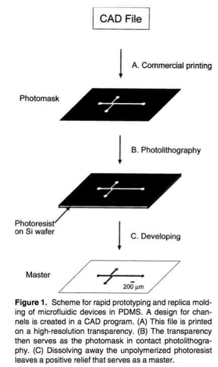
As mentioned in previous session, microfluidic device has long known to be made by photolithography technique. There are several reports of microfluidic systems based on PDMS.4 One of the system is called CE system.<sup>3</sup> The channels in PDMS was made by casting the polymer against a commercially obtained master that was composed of a positive relief structure of silicon.However, the devices were not sealed tightly.<sup>3</sup> In the following work, another method using a combination of high-resolution printing and contact photolithography process was created.<sup>3</sup> This technique has been described previously and has been used to generate a variety of microstructures with dimensions >20 μm.<sup>4</sup><sup>5</sup> The process is shown in the following figure.<sup>3</sup> | As mentioned in previous session, microfluidic device has long known to be made by photolithography technique. There are several reports of microfluidic systems based on PDMS.4 One of the system is called CE system.<sup>3</sup> The channels in PDMS was made by casting the polymer against a commercially obtained master that was composed of a positive relief structure of silicon.However, the devices were not sealed tightly.<sup>3</sup> In the following work, another method using a combination of high-resolution printing and contact photolithography process was created.<sup>3</sup> This technique has been described previously and has been used to generate a variety of microstructures with dimensions >20 μm.<sup>4</sup><sup>5</sup> The process is shown in the following figure.<sup>3</sup> | ||
[[Image:Example.jpg]] | |||
Revision as of 19:04, 26 March 2017
Overview of Photolithography
Photolithography is the process of transferring patterns using light. Usually, the light is used to transfer a geometric pattern from a photomask to a substrate. In the process of transfer, a series of chemical treatment happened to engrave desired patter on to substrate by photo resist.There are four basic steps in photolithography process, spin coating, pre-exposure bake, exposure to UV through the mask and post-exposure baking. In the first step. The wafer is covered with photoresist, which is a viscous liquid solution. To produce a uniform photoresist layer by spin coating. Usually, the spin coating runs around 3000rpm for one minute. The thickness of the photoresist layer is around 1 micrometer. The second step is heating the coated photoresist at 120 degree for five minutes to remove solvent and make the photoresist solidified on the wafer. Then, expose a pattern of intense light to the wafer. The light exposure causes chemical change which make some of the photoresist removable by chemical solution. After removing the some photoresist part, the rest needs to be reheating again to make the rest photoresist part stable.
Depends on the application, it has two mechanisms.
• Positive Photoresist, exposed region is soluble
The mechanism of positive photoresist is to change the chemical composition in exposed region, which increase the solubility of exposed area dramatically. The positive photoresist will give a higher resolution, ability to modify sidewall profile, easy to clean off a wafer and good plasma resistance for etching
• Negative Photoresist, unexposed region is soluble.
The mechanism of negative photoresist is to initiate cross-linking between polymer chains in exposed region. The negative photoresist will give high aspect ratio features, chemically resistant to organic solvents, patterning thick resists and relatively inexpensive material.
Photolithography Application
Photolithography technique has been used in making variety of devices, like electronic device, biosensor and microfluidic device. Due to recent report, fabrication techniques that have emerged from development efforts in photolithography.1 Photolithography in general, has three applications, fabricating stamps and molds, solid objective printing and three-dimensional nanofabrication using a conformable photomask.1 In the application of fabrication technique, people have been using rapid prototyping for a device in a computer aided design (CAD) program.2 The process contains producing a positive relief of photoresist on silicon wafer. In the following figure, obtained from McDonald's work, It illustrates how rapid prototyping works.2
To be more specific, micro contact printing has been used with the principle of photolithography. Microcontact printing (mCP) is a flexible, non-photolithographic method that routinely forms patterned SAMs containing regions terminated by different chemical functionalities with submicron lateral dimensions.1 The procedure is in the following figure.1
As mentioned in previous session, microfluidic device has long known to be made by photolithography technique. There are several reports of microfluidic systems based on PDMS.4 One of the system is called CE system.3 The channels in PDMS was made by casting the polymer against a commercially obtained master that was composed of a positive relief structure of silicon.However, the devices were not sealed tightly.3 In the following work, another method using a combination of high-resolution printing and contact photolithography process was created.3 This technique has been described previously and has been used to generate a variety of microstructures with dimensions >20 μm.45 The process is shown in the following figure.3


