Nanoimprint Lithography (NIL) - Carter Paul
Motivation
Nanostructures are an extremely important building block for the microchip, microelectronic, and biosensor industries to name a few. Research on nanostructures featuring high yield, precision, and low cost fabrication has been highly regarded in the nanotechnology industry. Fabrication techniques are paramount to the commercialism of nanotechnology, as the demand for products like semiconductor devices grows. In the 1990’s, nanostructure fabrication was completed via scanning probe microscope (SPM) lithography. This new technology was limited due to low throughput and was not produced outside of laboratory scale. At the time, X-ray lithography and extreme ultraviolet (EUV) lithography remained popular methods but were ultimately limited by material/equipment expenses.[1]
Introduction to NIL
Production scale-up of nanostructure materials/devices was first made possible in 1996 at the NanoStructure Laboratory at the University of Minnesota by Professor Stephen Y. Chou, who published his first paper on the topic that same year. Nanoimprint lithography (NIL) is known as the first feasible nanopatterning process at large scale. The overall end-product of NIL is the successful transfer of patterns of a given sample (such as a mold) to a substrate.[1] This mechanism is typically achieved through mechanical contact, heating, curing, or electrochemical reaction. NIL processes are fast at large scale and low cost compared to other lithography methods, an optimal choice for companies looking to scale up component production. These techniques, while fast and efficient, do not lack resolution. Patterns around a resolution of 5 nm can be readily achieved. The primary limiting factor for resolution is typically the mold used. Manufacturers of semiconductors and hard disk drives primarily utilize NIL as an alternative to photolithography. Other notable products that require NIL-produced nanostructures include light emitting devices, memory devices, solar cells, and even flash memory devices.[1] The semiconductor industry prioritizes NIL to manufacture smaller transistors and higher-density integrated circuits. NIL can also imprint functional device structures in various polymers, which can lead to a wide range of applications in electronics, photonics, data storage, and biotechnology.[2]
The principle of nanoimprinting is simple and efficient. A hard mold with nano-scale surface relief features is pressed into a chosen polymer cast on a substrate. Temperature and pressure are controlled within the environment throughout the entirety of each step of the process. A thin residual layer of polymer material is left behind underneath the mold and provides a layer of protection against the hard mold material on the substrate. This protects the nanoscale features on the mold surface, which are typically fragile. After a photocuring or hardening process, the removed mask material leaves behind the desired imprinted polymer pattern. A dry etching process is typically used to refine the pattern definition and remove the residual layer (if needed) once this process is complete. The mask and imprinting fluid material are dependent upon the application.[2][3]
Thermal NIL Process

Thermal NIL depends on the mechanical molding of polymers, which differs greatly from other lithography techniques. Although NIL does possess advantages allowing for viable scale-up, there are also defect control challenges that arise from process methods. In the process of thermal NIL, a mold with the correct feature size is pressed on a thermoplastic material substrate. This substrate is heated beforehand as part of the molding process. It is advantageous for the material temperature to exceed its glass transition temperature, in this case the polymer will behave as a viscous fluid which better facilitates the molding process.[1]
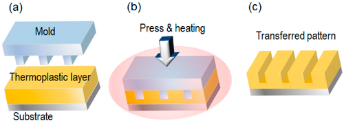
Figure 1 illustrates the thermal NIL process employing a planar mold created through electron beam lithography on silicon wafers. Initially, a thermoplastic layer was applied to a silicon substrate via spin-coating. Subsequently, the substrate was overlaid with the mold and heated to the mold's glass transition temperature, causing the thermoplastic layer to conform to the mold's shape. The mold and substrate were then cooled to below the glass transition temperature, solidifying the thermoplastic. Finally, the mold was separated from the substrate, leaving behind a patterned thermoplastic layer. A residual layer remains beneath the pattern, requiring removal via plasma etching for lift-off and an additional etching process for the substrate.[4]
Roll-to-roll Thermal NIL

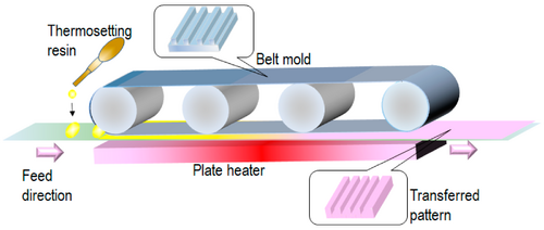
The throughput of thermal NIL can be increased by introducing a roll-to-roll web system. Thermoplastic films are flexible and compatible with the web system. The throughput (although increased) is limited by the time required for heating/cooling. Cameras are used to monitor the transferred patterns. In an attempt to improve the transferred pattern quality as well as throughput, a belt-type thermal NIL process has also been proposed (Figure 2). This type of system would use a thermosetting resin like polydimethylsiloxane (PDMS) and plate heater to cure the resin. A flexible polyurethane acrylate material would be an advantageous material for a mold. Contact between the heater and base film is not necessary because the tension of the film facilitates the contact between the belt mold. In this type of system, the cooling process is essential due to the risk of the imprinted pattern being released above its glass transition temperature. This condition would cause the pattern to dissipate immediately. High throughput is dependent on additional cooling apparatus to neutralize this risk.[4]
NIL Mold
The two main components required for NIL are a mold with pre-defined surface relief nanostructures and a suitable resist material that can be deformed and hardened to maintain the shape of an impression. The resist material can be a thermoplastic cured either thermally or by UV, this material is typically applied on top of a substrate. A NIL mold is required to be a solid material with high strength and durability. The molds are typically made in silicon (dielectric material), metals, or polymer materials with sufficient tensile properties. These property requirements are similar to those of elastomeric stamps used in soft lithography. These materials are essential to achieve nanoscale features due to the need for protrusion patterns on the mold to resist deformity during the imprinting process (especially at higher temperatures). These considerations allow for the preservation of pattern definition (independent of shape and aspect ratio) at scales as low as 5-10 nm.[2]
NIL Resist
Imprint lithography replicates surface relief patterns by mechanical embossing, therefore resist materials used in importing must be easy to deform under an applied pressure. Mechanical strengh is also important in order for the material to maintain structural integrity during the de-molding process. Two key material properties play a crucial role in the imprinting process. Firstly, the resist material must have a Young’s modulus lower than that of the mold during imprinting. This ensures that the resist material can be deformed by the mold. Secondly, the minimal pressure required for the imprint should exceed the shear modulus of the polymer. Additionally, the resist material should possess a sufficiently low viscosity to complete the imprinting process within a practical time frame. This viscosity requirement can be likened to the squeezed flow of a Newtonian liquid between plates with a radius R and a gap distance of d.[2]
Thermal NIL Resist
For materials used in the thermal NIL process, temperature must be raised above the materials glass transition temperature in order for the Young’s modulus to decrease and allow for molding. This process typically requires a 70-90°C increase above the glass transition temperature to increase material (polymer) viscosity. Following this, the mold and imprinted polymer must be cooled below the same glass transition temperature to achieve a desired pattern.[2]
The glass transition temperature represents the temperature at which chain motion becomes significant in polymers. Intermolecular forces and steric hindrance (crosslinking and/or branching) have the potential to increase this glass transition temperature value. These properties are exploited while choosing the optimal imprint resist material. It is desirable in most applications to use a lower temperature. Thermally curable or thermosetting polymers are considered excellent resist systems for thermal NIL. This is due to their capability to undergo crosslinking via thermal treatment, allowing for low-pressure imprinting and increased mechanical integrity post-curing.[2]
UV-NIL Resist
UV-NIL resists utilize similar materials (liquid precursors) that can be cured by UV light at ambient temperatures. These materials already possess a low Young’s modulus and viscosity. The low viscosity allows for the imprinting step to be less sensitive to any effects rising from the desired pattern density. The small area requirement for the mold allows for a continuous process on a larger substrate (roll-to-roll nanoimprinting).[2]
Ultraviolet (UV) NIL and Machining Mechanism

UV light has previously been used to create structures at the nano/micro level on photoresist material. This material is exposed to a UV light source which facilitates a chemical reaction. This way, the sample is developed to extract a desired pattern, which can even be scaled up to a batch and even continuous process. A method of UV lithography integration with continuous roll nanoimprinting has been developed to scale up production. A dispensing unit is used to provide a substrate with UV-curable polymer material. The polymer covered substrate then enters into the range of a UV illumination unit while also being contacted by a pattern rollerstamper. As the substrate passes through the stamper, the UV light hits the curing region which initiates pattern development. Substrates can either be rigid or flexible depending on the application and manufacturing unit available.[1]
Roll-to-roll NIL Fabrication Example
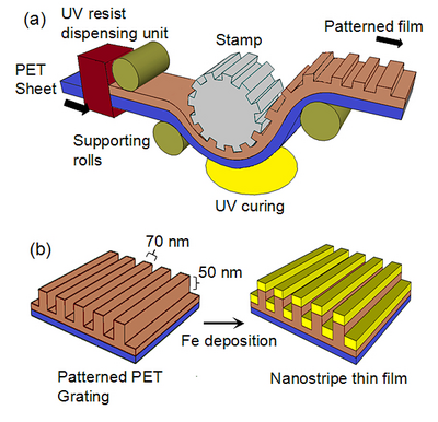
In Figure 3, roll-to-roll NIL is utilized to fabricate magnetic thin films on a flexible substrate. High density iron nano stripes were placed on 70 nm wide embossed polyethylene terephthalate (PET) sheets which served as a flexible substrate. The objective of this experiment was to determine the impact of film thickness on the magnetic properties of the sheet. Magnetic anisotropy properties were also recorded. These findings contribute to the potential application of magnetic nano stripes in flexible electronics for biomedical devices. [6]
References
[1] Wu, D.; S. Rajput, N.; Luo, X. Nanoimprint Lithography - the Past, the Present and the Future. Current Nanoscience 2016, 12 (6), 712–724. https://doi.org/10.2174/1573413712666160530120432
[2] Guo, L. J. Nanoimprint Lithography: Methods and Material Requirements. Advanced Materials 2007, 19 (4), 495–513. https://doi.org/10.1002/adma.200600882
[3] Traub, M.; Longsine, W.; Truskett, V. Advances in Nanoimprint Lithography. Annual Review of Chemical and Biomolecular Engineering 2016. https://doi.org/10.1146/annurev-chembioeng-080615-034635
[4] Unno, N.; Mäkelä, T. Thermal Nanoimprint Lithography—a Review of the Process, Mold Fabrication, and Material. Nanomaterials 2023, 13 (14), 2031. https://doi.org/10.3390/nano13142031
[5] Cox, L. M.; Martinez, A. M.; Blevins, A. K.; Sowan, N.; Ding, Y.; Bowman, C. N. Nanoimprint Lithography: Emergent Materials and Methods of Actuation. Nano Today 2020, 31, 100838. https://doi.org/10.1016/j.nantod.2019.100838
[6] Thantirige, R. M.; John, J.; Pradhan, N. R.; Carter, K. R.; Tuominen, M. T. Fabrication of Flexible Oriented Magnetic Thin Films with Large In-Plane Uniaxial Anisotropy by Roll-To-Roll Nanoimprint Lithography. Journal of magnetism and magnetic materials 2016, 407, 273–278. https://doi.org/10.1016/j.jmmm.2015.12.086
